- Courses
- Tutorials
- Interview Prep
GATE EC||ANALOG ELECTRONIC||CURRENT MIRROR CIRCUIT||PYQS(2000-2025)
Question 1
For the circuit shown in the following figure, transistors M1 and M2 are identical NMOS transistors. Assume that M2 is in saturation and the output is unloaded
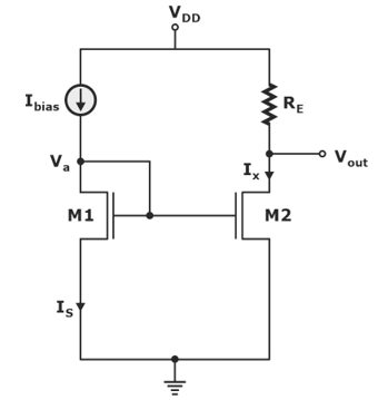
The current Ix is related to Ibias as
(GATE 2008 || EC || PYQ || MCQ || 2 MARKS)
IX = Ibias - IS
IX = Ibias
IX = Ibias – IS
Ix = Ibias − ((VDD − Vout) / RE)
Question 2
In the silicon BJT circuit shown below, assume that the emitter area of transistor Q1 is half that of transistor Q2.
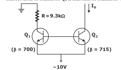
The value of current I0 is approximately
(GATE 2010 || EC || PYQ || MCQ || 1 MARKS)
0.5 mA
2 mA
9.3 mA
15 mA
Question 3
Resistor R1 in the circuit below has been adjusted so that I1 = 1 mA. The bipolar transistors Q1 and Q2 are perfectly matched and have very high current gain, so their base currents are negligible. The supply voltage Vcc is 6 V. The thermal voltage kT/q is 26 mV.
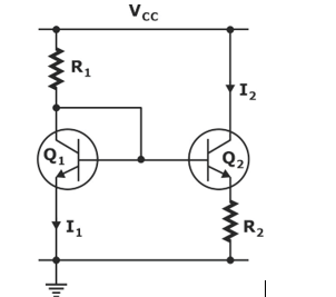
The value of R2 (in Ω) for which I2 = 100 μA is.
(GATE 2016 || EC || PYQ || NAT ||1 MARKS)
575.6
Question 4
In the circuit shown, V1 = 0 and V2 = Vdd. The other relevant parameters are mentioned in the figure. Ignoring the effect of channel length modulation and the body effect, the value of Iout is ___________ mA (rounded off to 1 decimal place).
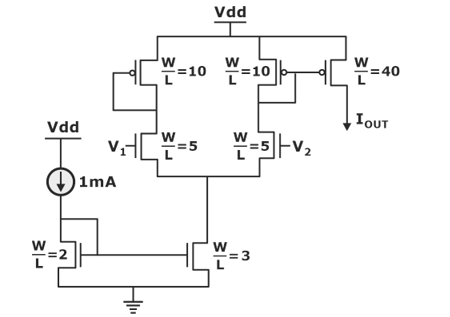
(GATE 2019 || EC || PYQ || NAT ||2 MARKS)
6
Question 5
In a simple MOS current mirror, channel length modulation causes:
(GATE 2012 || EC || PYQ || MCQ || 1 MARKS)
Zero output resistance
Output current independent of output voltage
Output current to vary with output voltage
Threshold voltage to become zero
Question 6
In a current mirror, the minimum output voltage required to keep MOSFET in saturation is called:
(GATE 2016 || EC || PYQ || MCQ || 1 MARKS)
Threshold voltage
Early voltage
Pinch-off voltage
Compliance voltage
Question 7
For an ideal current mirror, the output resistance should be:
(GATE 2021 || EC || PYQ || MCQ || 1 MARKS)
Infinite
Equal to load resistance
Zero
Low
There are 7 questions to complete.
